
PaRaDeSEC
Expanding Potential in Particle and Radiation Detectors, Sensors and Electronics in Croatia
Horizon 2020 - The EU Framework Programme for Research and Innovation

Horizon 2020 - The EU Framework Programme for Research and Innovation
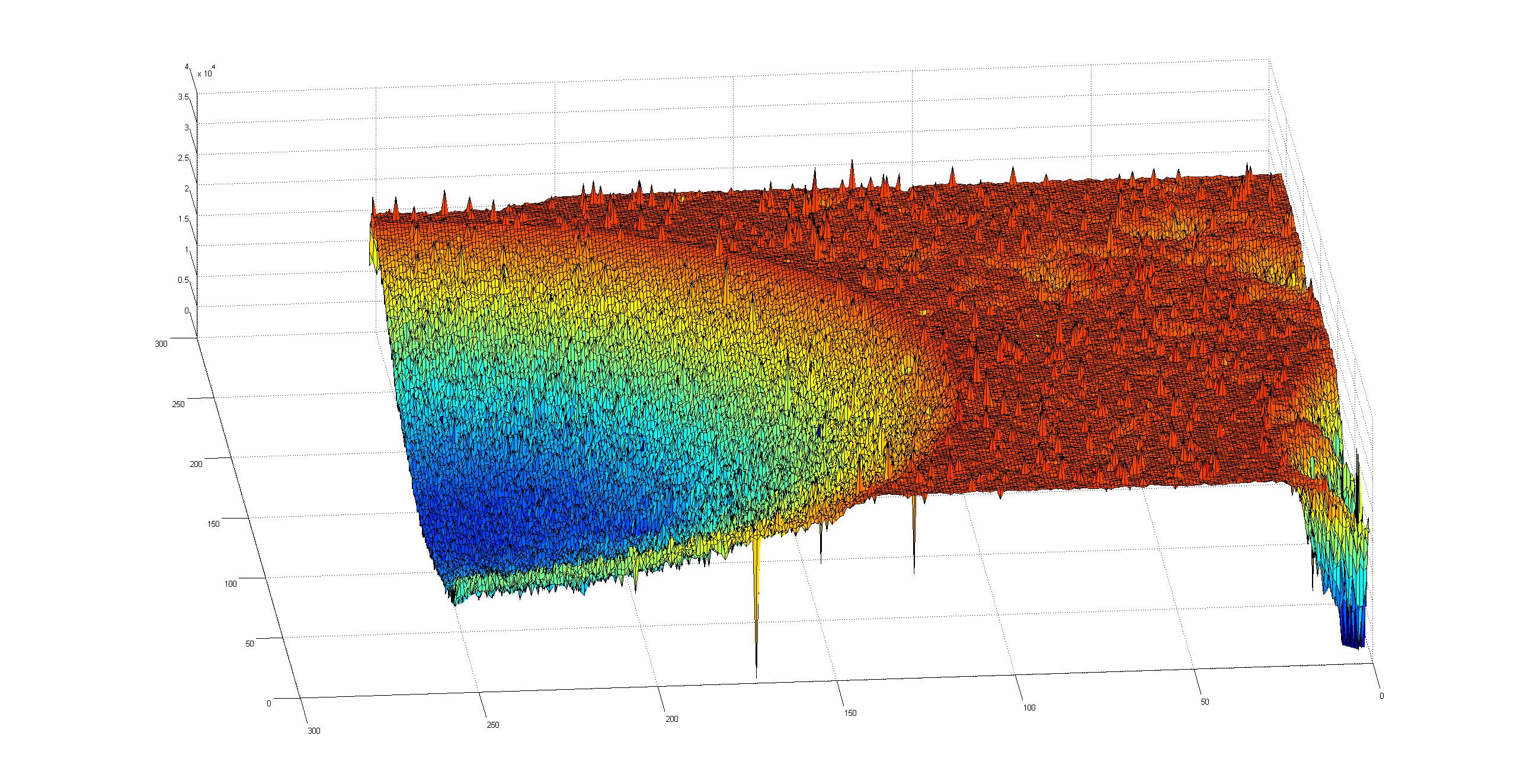
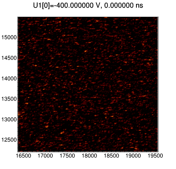
Semiconductor detectors are widely used in high-energy physics (HEP) experiments, nuclear safety monitoring, space missions and in various medical applications. Silicon pixel and microstrip detectors provide very precise spatial resolution while being cost-effective due to well-established semiconductor manufacturing technology. We have large interest on applications of a new processing technology, Atomic Layer Deposition (ALD), which provides significant potential for improve the performance of semiconductor detectors. The development of advanced radiation detectors is closely related with scientific activities of RBI Division of Materials Physics having a large variety of characterization and spectroscopy tools for semiconductor materials.
Internationally, there is close collaboration between e.g. R&D groups of CERN RD50 Collaboration, Micronova Center operated by Aalto University /VTT (Technical Research Centre of Finland Ltd) and CMS (Compact Muon Solenoid) experiment within the CERN LHC accelerator. The topics include e.g. p-type MCz-Si pixel sensors for CMS Phase II Upgrade and pixelated X-ray detectors made of different semiconductor materials, intended to be used for nuclear safety and medical applications.
Grant Agreement number: 669014
Approved after call H2020-WIDESPREAD-2014-2015/H2020-WIDESPREAD-2014-2
Start date: July 1st 2015. End date: March 31st 2021.
Total project funding: 2 705 000 €, EC contribution: 2 434 500 €